
The telecommunications industry has experienced tremendous growth over the past few decades, driven by the increasing demand for faster data transmission, reliable connectivity, and advanced communication technologies. From mobile networks and fiber-optic infrastructure to satellite communication and 5G systems, telecommunications equipment relies heavily on high-performance electronic assemblies. At the heart of these systems is telecom PCB assembly, a critical manufacturing process that ensures communication devices operate efficiently, reliably, and continuously.
As network infrastructures become more complex and data traffic continues to increase, telecom PCB assembly plays an increasingly important role in supporting the global communication ecosystem. Understanding its manufacturing process, benefits, requirements, and applications can help businesses appreciate its significance in modern telecommunications.
What Is Telecom PCB Assembly?
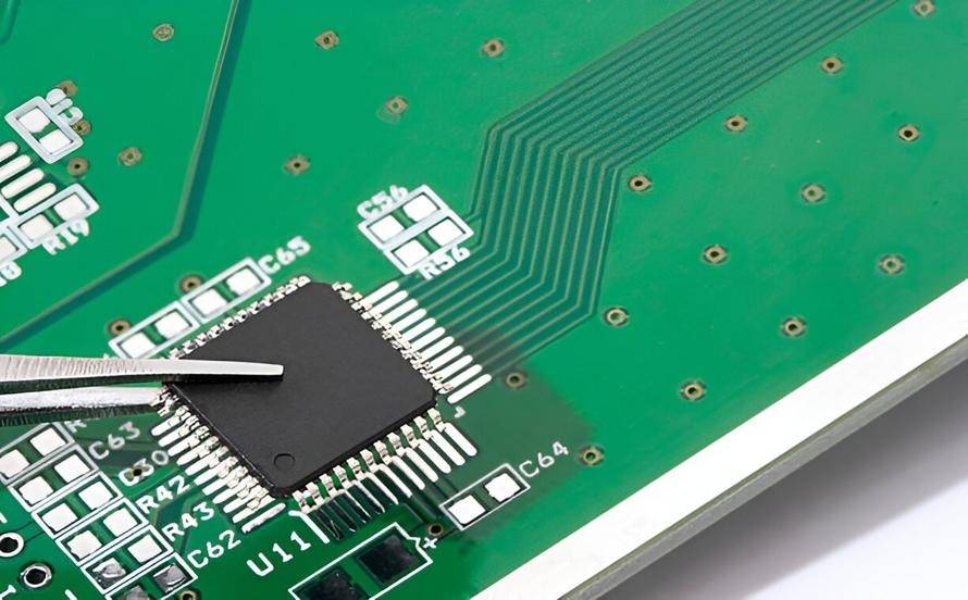
Telecom PCB assembly refers to the process of assembling electronic components onto printed circuit boards specifically designed for telecommunications equipment. These circuit boards serve as the foundation for various communication devices, enabling signal processing, data transmission, network management, and wireless connectivity.
Telecommunications PCBs are used in equipment such as routers, switches, base stations, antennas, signal amplifiers, satellite communication systems, optical networking devices, and wireless communication modules.
Unlike standard PCB assemblies, telecom PCBs often require high-frequency performance, superior signal integrity, excellent reliability, and the ability to operate continuously under demanding environmental conditions.
Because communication systems form the backbone of modern society, telecom PCB assemblies must meet strict quality and performance standards.
Importance of Telecom PCB Assembly
The importance of telecom PCB assembly extends across nearly every aspect of modern communication. Whether enabling mobile phone calls, internet connectivity, cloud computing, or video streaming services, telecom equipment depends on reliable electronic assemblies.
Telecommunication networks operate around the clock, requiring equipment that can deliver uninterrupted performance. Any failure within a communication system can lead to service disruptions, financial losses, and reduced customer satisfaction.
High-quality telecom PCB assembly helps ensure network reliability, signal accuracy, and long-term operational stability. It also supports emerging technologies such as 5G, Internet of Things (IoT), artificial intelligence, and edge computing.
As communication demands continue to grow, the role of advanced PCB assembly becomes even more critical.
Key Requirements of Telecom PCB Assembly
A successful telecom PCB assembly must meet several technical requirements to support modern communication systems.
Signal integrity is one of the most important considerations. Telecommunications equipment often operates at high frequencies, making precise signal transmission essential. PCB layouts must minimize signal loss, crosstalk, and electromagnetic interference.
Reliability is another crucial requirement. Telecom equipment frequently operates in challenging environments and must function continuously for extended periods without failure.
Thermal management is equally important. Many communication devices generate significant heat, requiring efficient heat dissipation solutions to maintain stable operation.
Power integrity must also be maintained to ensure consistent voltage delivery and minimize electrical noise.
Additionally, telecom PCB assemblies often require compliance with industry standards and regulatory requirements to ensure safety and performance.
Materials Used in Telecom PCB Assembly
Material selection plays a significant role in the performance of telecom PCB assembly products.
Standard FR4 materials may be suitable for some communication applications, but high-frequency systems often require specialized substrates. Materials such as Rogers, PTFE, and other low-loss laminates are commonly used to support high-speed signal transmission.
Copper thickness and surface finishes are carefully selected to optimize conductivity and reliability.
Thermal management materials may be incorporated to improve heat dissipation, particularly in high-power communication equipment.
The choice of materials depends on factors such as operating frequency, environmental conditions, power requirements, and overall system performance objectives.
Telecom PCB Assembly Manufacturing Process
The manufacturing process for telecom PCB assembly involves multiple stages designed to ensure precision and quality.
The process begins with design verification and engineering review. Design files, bills of materials, and assembly requirements are carefully evaluated to identify potential manufacturing challenges.
PCB fabrication is completed according to the specified design and material requirements. Once the bare boards are ready, solder paste is applied to component pads using precision stencil printing.
Surface-mount technology (SMT) equipment then places components onto the PCB with high accuracy. Through-hole components may be added using automated or manual assembly techniques when necessary.
The assembled boards pass through reflow soldering ovens, where controlled heating profiles create reliable solder joints.
Inspection and testing follow assembly. Automated Optical Inspection (AOI), X-ray inspection, in-circuit testing, and functional testing help verify quality and performance.
These manufacturing steps ensure that telecom PCB assemblies meet the demanding requirements of communication systems.
Advantages of Telecom PCB Assembly
One of the primary benefits of telecom PCB assembly is enhanced reliability. Telecommunications networks depend on equipment that can operate continuously with minimal downtime, and high-quality PCB assemblies help achieve this goal.
Another advantage is improved signal performance. Advanced assembly techniques and materials support high-speed data transmission while minimizing signal degradation.
Telecom PCB assemblies also enable compact and efficient equipment designs. As communication devices become more powerful, manufacturers must integrate increasing functionality into smaller spaces.
Scalability is another key benefit. Telecom PCB assembly supports production volumes ranging from prototypes to large-scale manufacturing, allowing companies to adapt to changing market demands.
Additionally, modern assembly technologies help reduce manufacturing defects, improve product consistency, and lower overall production costs.
Applications of Telecom PCB Assembly
The applications of telecom PCB assembly span a wide range of communication technologies and infrastructure.
Mobile communication systems rely on telecom PCB assemblies in base stations, signal amplifiers, antennas, and radio frequency modules. These systems enable wireless communication for billions of users worldwide.
Networking equipment such as routers, switches, gateways, and network servers uses telecom PCB assemblies to manage and transmit data efficiently.
Fiber-optic communication systems depend on specialized PCB assemblies for signal processing, transmission, and network management.
Satellite communication equipment utilizes telecom PCB assemblies to support reliable communication across vast distances.
Data centers also rely heavily on telecom PCB assemblies in servers, storage systems, and networking hardware that support cloud computing and digital services.
Emerging technologies such as 5G infrastructure, IoT devices, and smart city systems further expand the applications of telecom PCB assembly.
Quality Control in Telecom PCB Assembly
Quality assurance is essential in telecom PCB assembly because communication equipment must maintain consistent performance and reliability.
Manufacturers implement comprehensive inspection procedures throughout the production process. Automated Optical Inspection systems detect component placement errors, soldering defects, and assembly inconsistencies.
X-ray inspection is used to evaluate hidden solder joints, particularly in ball grid array (BGA) components and high-density assemblies.
Electrical testing verifies circuit continuity and component functionality.
Functional testing simulates real-world operating conditions to ensure that assembled boards perform as intended.
Traceability systems track materials, components, and manufacturing processes, supporting quality management and regulatory compliance.
These measures help ensure that telecom PCB assemblies meet the highest industry standards.
Future Trends in Telecom PCB Assembly
The future of telecom PCB assembly is closely tied to advancements in communication technology. The global rollout of 5G networks is increasing demand for high-frequency PCB assemblies capable of supporting faster data rates and lower latency.
Artificial intelligence and machine learning are being integrated into communication infrastructure, requiring more powerful and sophisticated electronic assemblies.
The expansion of IoT ecosystems is driving the development of compact, energy-efficient communication devices.
Advanced materials, automated manufacturing technologies, and intelligent quality control systems will continue to improve telecom PCB assembly capabilities in the years ahead.
Conclusion
Telecom PCB assembly is a vital component of modern communication infrastructure, enabling reliable connectivity, high-speed data transmission, and advanced networking capabilities. From mobile networks and fiber-optic systems to satellite communications and data centers, telecom PCB assemblies support the technologies that keep the world connected.
As communication networks continue to evolve and expand, the demand for high-quality telecom PCB solutions will only increase. Companies seeking reliable performance, advanced manufacturing capabilities, and consistent quality often partner with a trusted telecom PCB assembly service provider to ensure the success of their communication products and infrastructure projects.